Spectroscopy
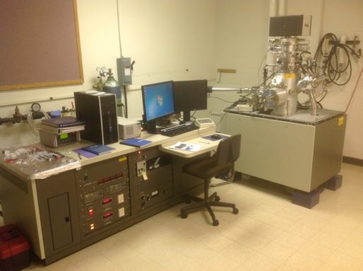
Auger Electron Nanoprobe
Our Physical Electronics 680 scanning Auger nanoprobe was designed for rapid, spatially resolved elemental and chemical analysis of solid surfaces, the main features are:
• Quantitative analysis of elements except hydrogen and helium
• Typical element detection limits are 0.1 atomic% from the top few nm
• SEM (scanning electron microscopy)
• SAM (scanning Auger microprobe) allows surface chemical maps to be collected with lateral resolutions better than 100 nm.
• Chemical state information of certain elements (particularly Al, Mg, Si etc.) can be obtained
• Sputter depth profiling reveals chemical depth information.
Typical Applications
• Microscopic particle identification
• Passive oxide film thickness
• Contamination on integrated circuits
• Quantification of light element surface films
• Mapping spatial distribution of surface constituents
Limitations
• Range of elements: All except H and He
• Samples can be conductors and semiconductors. Analysis of insulators is difficult but possible
•Lateral Resolution: 10- 30 nm for Auger analysis and even less for imaging
• Sampling depth: 0.5- 10 nm
• Detection limits: 0.1- 1 at%
• Accuracy: ± 30% if using published elemental sensitivity
± 10% if using standards that closely resemble the sample
Sample Requirements
Samples should be no larger than approximately 3/4 in. by 1/2 in. (18 mm by 12 mm). Height of samples should not exceed 1/2 in. (12mm). Samples must be conductive or area of interest must be properly grounded. Insulating samples, including thick insulating films (>30 nm), cannot be analyzed. Samples must also be compatible with a high vacuum environment (<1x10⁻⁹ Torr). Samples can be conductors and semiconductors. Analysis of insulators is difficult but possible.


Auger Electron Spectroscopy (AES) provides information about the chemical composition of the outermost material surface. The advantages of AES over other surface analysis methods are excellent spatial resolution (<1µm), surface sensitivity (~2nm), and detection of light elements. Detection limits for most elements range from about 0.01 to 0.1 at%.
Underlying the spectroscopic technique is the Auger effect. AES uses a high energy (1-20 keV) electron beam to excite the sample surface. When an inner-shell electron is ejected from a sample atom by the interaction with a primary electron, an electron from an outer shell fills the vacancy. To compensate for the energy change from this transition, an Auger electron or an x-ray is emitted. For light elements, the probability is greatest for the emission of an Auger electron, which accounts for the light-element sensitivity technique. The energy of the emitted Auger electron is characteristic of the element from which it was emitted. Detection and energy analysis of the emitted Auger electrons produces a spectrum of Auger electron energy versus the relative abundance of electrons. Peaks in the spectrum identify the elemental composition of the sample surface. In some cases, the chemical state of the surface atoms can also be determined from energy shifts and peak shapes.
Auger electrons have relatively low kinetic energy, which limits their escape depth. Any Auger electrons emitted from an interaction below the surface will lose energy through additional scattering electrons along its path to the surface and reach the detector. Auger electrons emitted at a depth greater than about 2-3 nm will not have sufficient energy to escape the surface and reach the detector. Thus, the analysis volume for AES extends only to a depth of about 2 nm. However, it is important to know that the analysis depth is not affected by the electron energy impinging the sample surface.